Nanotechnology ("nanotech") is the manipulation of matter on an
atomic,
molecular, and
supramolecular scale. The earliest, widespread description of nanotechnology
[1][2] referred to the particular technological goal of precisely manipulating atoms and molecules for fabrication of macroscale products, also now referred to as
molecular nanotechnology. A more generalized description of nanotechnology was subsequently established by the
National Nanotechnology Initiative, which defines nanotechnology as the manipulation of matter with at least one dimension sized from 1 to 100
nanometers. This definition reflects the fact that
quantum mechanical effects are important at this
quantum-realm scale, and so the definition shifted from a particular technological goal to a research category inclusive of all types of research and technologies that deal with the special properties of matter that occur below the given size threshold. It is therefore common to see the plural form "nanotechnologies" as well as "nanoscale technologies" to refer to the broad range of research and applications whose common trait is size. Because of the variety of potential applications (including industrial and military), governments have invested billions of dollars in nanotechnology research. Through its National Nanotechnology Initiative, the USA has invested 3.7 billion dollars. The European Union has invested
[when?] 1.2 billion and Japan 750 million dollars.
[3]
Scientists currently debate the future
implications of nanotechnology. Nanotechnology may be able to create many new materials and devices with a vast range of
applications, such as in
medicine,
electronics,
biomaterials energy production, and consumer products. On the other hand, nanotechnology raises many of the same issues as any new technology, including concerns about the
toxicity and environmental impact of nanomaterials,
[5] and their potential effects on global economics, as well as speculation about various
doomsday scenarios. These concerns have led to a debate among advocacy groups and governments on whether special
regulation of nanotechnology is warranted.
Origins[edit]
The concepts that seeded nanotechnology were first discussed in 1959 by renowned physicist
Richard Feynman in his talk
There's Plenty of Room at the Bottom, in which he described the possibility of synthesis via direct manipulation of atoms. The term "nano-technology" was first used by
Norio Taniguchi in 1974, though it was not widely known.

Comparison of Nanomaterials Sizes
Inspired by Feynman's concepts,
K. Eric Drexler used the term "nanotechnology" in his 1986 book
Engines of Creation: The Coming Era of Nanotechnology, which proposed the idea of a nanoscale "assembler" which would be able to build a copy of itself and of other items of arbitrary complexity with atomic control. Also in 1986, Drexler co-founded
The Foresight Institute (with which he is no longer affiliated) to help increase public awareness and understanding of nanotechnology concepts and implications.
Thus, emergence of nanotechnology as a field in the 1980s occurred through convergence of Drexler's theoretical and public work, which developed and popularized a conceptual framework for nanotechnology, and high-visibility experimental advances that drew additional wide-scale attention to the prospects of atomic control of matter. In 1980s two major breakthroughs incepted the growth of nanotechnology in modern era.

Buckminsterfullerene C60, also known as the buckyball, is a representative member of the carbon structures known as fullerenes. Members of the fullerene family are a major subject of research falling under the nanotechnology umbrella.
In the early 2000s, the field garnered increased scientific, political, and commercial attention that led to both controversy and progress. Controversies emerged regarding the definitions and potential implications of nanotechnologies, exemplified by the
Royal Society's report on nanotechnology.
[10] Challenges were raised regarding the feasibility of applications envisioned by advocates of molecular nanotechnology, which culminated in a public debate between Drexler and Smalley in 2001 and 2003.
[11]
Meanwhile, commercialization of products based on advancements in nanoscale technologies began emerging. These products are limited to bulk applications of
nanomaterials and do not involve atomic control of matter. Some examples include the
Silver Nano platform for using
silver nanoparticles as an antibacterial agent,
nanoparticle-based transparent sunscreens, and
carbon nanotubes for stain-resistant textiles.
[12][13]
Governments moved to promote and
fund research into nanotechnology, beginning in the U.S. with the
National Nanotechnology Initiative, which formalized a size-based definition of nanotechnology and established funding for research on the nanoscale.
By the mid-2000s new and serious scientific attention began to flourish. Projects emerged to produce nanotechnology roadmaps
[14][15] which center on atomically precise manipulation of matter and discuss existing and projected capabilities, goals, and applications.
Fundamental concepts[edit]
Nanotechnology is the engineering of functional systems at the molecular scale. This covers both current work and concepts that are more advanced. In its original sense, nanotechnology refers to the projected ability to construct items from the bottom up, using techniques and tools being developed today to make complete, high performance products.
One
nanometer (nm) is one billionth, or 10
−9, of a meter. By comparison, typical carbon-carbon
bond lengths, or the spacing between these
atoms in a
molecule, are in the range
0.12–0.15 nm, and a
DNA double-helix has a diameter around 2 nm. On the other hand, the smallest
cellular life-forms, the bacteria of the genus
Mycoplasma, are around 200 nm in length. By convention, nanotechnology is taken as the scale range
1 to 100 nm following the definition used by the National Nanotechnology Initiative in the US. The lower limit is set by the size of atoms (hydrogen has the smallest atoms, which are approximately a quarter of a nm diameter) since nanotechnology must build its devices from atoms and molecules. The upper limit is more or less arbitrary but is around the size that phenomena not observed in larger structures start to become apparent and can be made use of in the nano device.
[16] These new phenomena make nanotechnology distinct from devices which are merely miniaturised versions of an equivalent
macroscopic device; such devices are on a larger scale and come under the description of
microtechnology.
[17]
To put that scale in another context, the comparative size of a nanometer to a meter is the same as that of a marble to the size of the earth.
[18] Or another way of putting it: a nanometer is the amount an average man's beard grows in the time it takes him to raise the razor to his face.
[18]
Two main approaches are used in nanotechnology. In the "bottom-up" approach, materials and devices are built from molecular components which
assemble themselves chemically by principles of
molecular recognition. In the "top-down" approach, nano-objects are constructed from larger entities without atomic-level control.
[19]
Larger to smaller: a materials perspective

Several phenomena become pronounced as the size of the system decreases. These include
statistical mechanical effects, as well as
quantum mechanical effects, for example the “
quantum size effect” where the electronic properties of solids are altered with great reductions in particle size. This effect does not come into play by going from macro to micro dimensions. However, quantum effects can become significant when the nanometer size range is reached, typically at distances of 100 nanometers or less, the so-called
quantum realm. Additionally, a number of physical (mechanical, electrical, optical, etc.) properties change when compared to macroscopic systems. One example is the increase in surface area to volume ratio altering mechanical, thermal and catalytic properties of materials. Diffusion and reactions at nanoscale, nanostructures materials and nanodevices with fast ion transport are generally referred to nanoionics.
Mechanical properties of nanosystems are of interest in the nanomechanics research. The catalytic activity of nanomaterials also opens potential risks in their interaction with
biomaterials.
Materials reduced to the nanoscale can show different properties compared to what they exhibit on a macroscale, enabling unique applications. For instance, opaque substances can become transparent (copper); stable materials can turn combustible (aluminum); insoluble materials may become soluble (gold). A material such as gold, which is chemically inert at normal scales, can serve as a potent chemical
catalyst at nanoscales. Much of the fascination with nanotechnology stems from these quantum and surface phenomena that matter exhibits at the nanoscale.
[20]
Simple to complex: a molecular perspective
Modern
synthetic chemistry has reached the point where it is possible to prepare small molecules to almost any structure. These methods are used today to manufacture a wide variety of useful chemicals such as
pharmaceuticals or commercial
polymers. This ability raises the question of extending this kind of control to the next-larger level, seeking methods to assemble these single molecules into
supramolecular assemblies consisting of many molecules arranged in a well defined manner.
These approaches utilize the concepts of molecular self-assembly and/or
supramolecular chemistry to automatically arrange themselves into some useful conformation through a
bottom-upapproach. The concept of molecular recognition is especially important: molecules can be designed so that a specific configuration or arrangement is favored due to
non-covalentintermolecular forces. The Watson–Crick
basepairing rules are a direct result of this, as is the specificity of an
enzyme being targeted to a single
substrate, or the specific
folding of the proteinitself. Thus, two or more components can be designed to be complementary and mutually attractive so that they make a more complex and useful whole.
Such bottom-up approaches should be capable of producing devices in parallel and be much cheaper than top-down methods, but could potentially be overwhelmed as the size and complexity of the desired assembly increases. Most useful structures require complex and thermodynamically unlikely arrangements of atoms. Nevertheless, there are many examples of self-assembly based on molecular recognition in
biology, most notably Watson–Crick basepairing and enzyme-substrate interactions. The challenge for nanotechnology is whether these principles can be used to engineer new constructs in addition to natural ones.
Molecular nanotechnology: a long-term view
Molecular nanotechnology, sometimes called molecular manufacturing, describes engineered nanosystems (nanoscale machines) operating on the molecular scale. Molecular nanotechnology is especially associated with the
molecular assembler, a machine that can produce a desired structure or device atom-by-atom using the principles of
mechanosynthesis. Manufacturing in the context of
productive nanosystems is not related to, and should be clearly distinguished from, the conventional technologies used to manufacture nanomaterials such as carbon nanotubes and nanoparticles.
When the term "nanotechnology" was independently coined and popularized by
Eric Drexler (who at the time was unaware of an
earlier usage by Norio Taniguchi) it referred to a future manufacturing technology based on
molecular machine systems. The premise was that molecular scale biological analogies of traditional machine components demonstrated molecular machines were possible: by the countless examples found in biology, it is known that sophisticated,
stochastically optimised biological machines can be produced.
It is hoped that developments in nanotechnology will make possible their construction by some other means, perhaps using
biomimetic principles. However, Drexler and other researchers
[21]have proposed that advanced nanotechnology, although perhaps initially implemented by biomimetic means, ultimately could be based on mechanical engineering principles, namely, a manufacturing technology based on the mechanical functionality of these components (such as gears, bearings, motors, and structural members) that would enable programmable, positional assembly to atomic specification. The physics and engineering performance of exemplar designs were analyzed in Drexler's book
Nanosystems.
In general it is very difficult to assemble devices on the atomic scale, as one has to position atoms on other atoms of comparable size and stickiness. Another view, put forth by Carlo Montemagno,
[23] is that future nanosystems will be hybrids of silicon technology and biological molecular machines. Richard Smalley argued that mechanosynthesis are impossible due to the difficulties in mechanically manipulating individual molecules.
This led to an exchange of letters in the
ACS publication
Chemical & Engineering News in 2003.
[24] Though biology clearly demonstrates that molecular machine systems are possible, non-biological molecular machines are today only in their infancy. Leaders in research on non-biological molecular machines are Dr.
Alex Zettl and his colleagues at Lawrence Berkeley Laboratories and UC Berkeley.
[citation needed] They have constructed at least three distinct molecular devices whose motion is controlled from the desktop with changing voltage: a nanotube
nanomotor, a molecular actuator, and a nanoelectromechanical relaxation oscillator. See
nanotube nanomotor for more examples.
An experiment indicating that positional molecular assembly is possible was performed by Ho and Lee at
Cornell University in 1999. They used a scanning tunneling microscope to move an individual carbon monoxide molecule (CO) to an individual iron atom (Fe) sitting on a flat silver crystal, and chemically bound the CO to the Fe by applying a voltage.
Current research
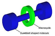
Graphical representation of a rotaxane, useful as a molecular switch.
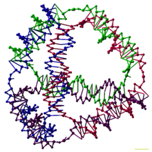
This DNA tetrahedron[27] is an artificially designed nanostructure of the type made in the field of DNA nanotechnology. Each edge of the tetrahedron is a 20 base pair DNA double helix, and each vertex is a three-arm junction.
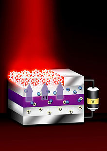
This device transfers energy from nano-thin layers of quantum wells to nanocrystals above them, causing the nanocrystals to emit visible light.[28]
Nanomaterials
The nanomaterials field includes subfields which develop or study materials having unique properties arising from their nanoscale dimensions.[29]
- Interface and colloid science has given rise to many materials which may be useful in nanotechnology, such as carbon nanotubes and other fullerenes, and various nanoparticles and nanorods. Nanomaterials with fast ion transport are related also to nanoionics and nanoelectronics.
- Nanoscale materials can also be used for bulk applications; most present commercial applications of nanotechnology are of this flavor.
- Progress has been made in using these materials for medical applications; see Nanomedicine.
- Nanoscale materials such as nanopillars are sometimes used in solar cells which combats the cost of traditional Silicon solar cells.
- Development of applications incorporating semiconductor nanoparticles to be used in the next generation of products, such as display technology, lighting, solar cells and biological imaging; see quantum dots.
Bottom-up approaches
These seek to arrange smaller components into more complex assemblies.
- DNA nanotechnology utilizes the specificity of Watson–Crick basepairing to construct well-defined structures out of DNA and other nucleic acids.
- Approaches from the field of "classical" chemical synthesis (Inorganic and organic synthesis) also aim at designing molecules with well-defined shape (e.g. bis-peptides[30]).
- More generally, molecular self-assembly seeks to use concepts of supramolecular chemistry, and molecular recognition in particular, to cause single-molecule components to automatically arrange themselves into some useful conformation.
- Atomic force microscope tips can be used as a nanoscale "write head" to deposit a chemical upon a surface in a desired pattern in a process called dip pen nanolithography. This technique fits into the larger subfield of nanolithography.
Top-down approaches
These seek to create smaller devices by using larger ones to direct their assembly.
Functional approaches
These seek to develop components of a desired functionality without regard to how they might be assembled.
Biomimetic approaches
Bionics or biomimicry seeks to apply biological methods and systems found in nature, to the study and design of engineering systems and modern technology. Biomineralization is one example of the systems studied.
Speculative
These subfields seek to anticipate what inventions nanotechnology might yield, or attempt to propose an agenda along which inquiry might progress. These often take a big-picture view of nanotechnology, with more emphasis on its societal implications than the details of how such inventions could actually be created.
- Molecular nanotechnology is a proposed approach which involves manipulating single molecules in finely controlled, deterministic ways. This is more theoretical than the other subfields, and many of its proposed techniques are beyond current capabilities.
- Nanorobotics centers on self-sufficient machines of some functionality operating at the nanoscale. There are hopes for applying nanorobots in medicine,[36][37][38] but it may not be easy to do such a thing because of several drawbacks of such devices.[39] Nevertheless, progress on innovative materials and methodologies has been demonstrated with some patents granted about new nanomanufacturing devices for future commercial applications, which also progressively helps in the development towards nanorobots with the use of embedded nanobioelectronics concepts.[40][41]
- Productive nanosystems are "systems of nanosystems" which will be complex nanosystems that produce atomically precise parts for other nanosystems, not necessarily using novel nanoscale-emergent properties, but well-understood fundamentals of manufacturing. Because of the discrete (i.e. atomic) nature of matter and the possibility of exponential growth, this stage is seen as the basis of another industrial revolution. Mihail Roco, one of the architects of the USA's National Nanotechnology Initiative, has proposed four states of nanotechnology that seem to parallel the technical progress of the Industrial Revolution, progressing from passive nanostructures to active nanodevices to complex nanomachines and ultimately to productive nanosystems.[42]
- Programmable matter seeks to design materials whose properties can be easily, reversibly and externally controlled though a fusion of information science and materials science.
- Due to the popularity and media exposure of the term nanotechnology, the words picotechnology and femtotechnology have been coined in analogy to it, although these are only used rarely and informally.
Tools and techniques

Typical AFM setup. A microfabricated cantileverwith a sharp tip is deflected by features on a sample surface, much like in a phonograph but on a much smaller scale. A laser beam reflects off the backside of the cantilever into a set of photodetectors, allowing the deflection to be measured and assembled into an image of the surface.
The tip of a scanning probe can also be used to manipulate nanostructures (a process called positional assembly).
Feature-oriented scanning methodology may be a promising way to implement these nanomanipulations in automatic mode. However, this is still a slow process because of low scanning velocity of the microscope.
Another group of nanotechnological techniques include those used for fabrication of
nanotubes and
nanowires, those used in semiconductor fabrication such as deep ultraviolet lithography, electron beam lithography, focused ion beam machining, nanoimprint lithography, atomic layer deposition, and molecular vapor deposition, and further including molecular self-assembly techniques such as those employing di-block copolymers. The precursors of these techniques preceded the nanotech era, and are extensions in the development of scientific advancements rather than techniques which were devised with the sole purpose of creating nanotechnology and which were results of nanotechnology research.
The top-down approach anticipates nanodevices that must be built piece by piece in stages, much as manufactured items are made. Scanning probe microscopy is an important technique both for characterization and synthesis of nanomaterials. Atomic force microscopes and scanning tunneling microscopes can be used to look at surfaces and to move atoms around. By designing different tips for these microscopes, they can be used for carving out structures on surfaces and to help guide self-assembling structures. By using, for example, feature-oriented scanning approach, atoms or molecules can be moved around on a surface with scanning probe microscopy techniques. At present, it is expensive and time-consuming for mass production but very suitable for laboratory experimentation.
In contrast, bottom-up techniques build or grow larger structures atom by atom or molecule by molecule. These techniques include chemical synthesis,
self-assembly and positional assembly.
Dual polarisation interferometry is one tool suitable for characterisation of self assembled thin films. Another variation of the bottom-up approach is
molecular beam epitaxy or MBE. Researchers at
Bell Telephone Laboratories like John R. Arthur. Alfred Y. Cho, and Art C. Gossard developed and implemented MBE as a research tool in the late 1960s and 1970s. Samples made by MBE were key to the discovery of the fractional quantum Hall effect for which the 1998 Nobel Prize in Physics was awarded. MBE allows scientists to lay down atomically precise layers of atoms and, in the process, build up complex structures. Important for research on semiconductors, MBE is also widely used to make samples and devices for the newly emerging field of
spintronics.
However, new therapeutic products, based on responsive nanomaterials, such as the ultradeformable, stress-sensitive
Transfersome vesicles, are under development and already approved for human use in some countries.
[citation needed]
Applications
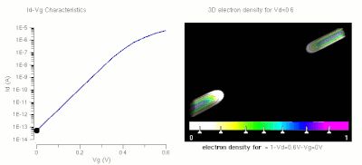
One of the major applications of nanotechnology is in the area of nanoelectronics with MOSFET's being made of small nanowires ~10 nm in length. Here is a simulation of such a nanowire.
As of August 21, 2008, the
Project on Emerging Nanotechnologies estimates that over 800 manufacturer-identified nanotech products are publicly available, with new ones hitting the market at a pace of 3–4 per week. The project lists all of the products in a publicly accessible online database. Most applications are limited to the use of "first generation" passive nanomaterials which includes titanium dioxide in sunscreen, cosmetics, surface coatings, and some food products; Carbon allotropes used to produce
gecko tape; silver in food packaging, clothing, disinfectants and household appliances; zinc oxide in sunscreens and cosmetics, surface coatings, paints and outdoor furniture varnishes; and cerium oxide as a fuel catalyst.
Further applications allow
tennis balls to last longer,
golf balls to fly straighter, and even
bowling balls to become more durable and have a harder surface.
Trousers and
socks have been infused with nanotechnology so that they will last longer and keep people cool in the summer.
Bandages are being infused with silver nanoparticles to heal cuts faster.
[46] Video game consoles and
personal computers may become cheaper, faster, and contain more memory thanks to nanotechnology.
[47] Nanotechnology may have the ability to make existing medical applications cheaper and easier to use in places like the
general practitioner's office and at home.
[48] Cars are being manufactured with
nanomaterials so they may need fewer
metals and less
fuel to operate in the future.
Scientists are now turning to nanotechnology in an attempt to develop diesel engines with cleaner exhaust fumes. Platinum is currently used as the diesel engine
catalyst in these engines. The catalyst is what cleans the exhaust fume particles. First a reduction catalyst is employed to take nitrogen atoms from NOx molecules in order to free oxygen. Next the oxidation catalyst oxidizes the hydrocarbons and carbon monoxide to form carbon dioxide and water. Platinum is used in both the reduction and the oxidation catalysts. Using platinum though, is inefficient in that it is expensive and unsustainable. Danish company InnovationsFonden invested DKK 15 million in a search for new catalyst substitutes using nanotechnology. The goal of the project, launched in the autumn of 2014, is to maximize surface area and minimize the amount of material required. Objects tend to minimize their surface energy; two drops of water, for example, will join to form one drop and decrease surface area. If the catalyst's surface area that is exposed to the exhaust fumes is maximized, efficiency of the catalyst is maximized. The team working on this project aims to create nanoparticles that will not merge together. Every time the surface is optimized, material is saved. Thus, creating these nanoparticles will increase the effectiveness of the resulting diesel engine catalyst—in turn leading to cleaner exhaust fumes—and will decrease cost. If successful, the team hopes to reduce platinum use by 25%.
Nanotechnology also has a prominent role in the fast developing field of
Tissue Engineering. When designing scaffolds, researchers attempt to the mimic the nanoscale features of a
Cell's microenvironment to direct its differentiation down a suitable lineage. For example, when creating scaffolds to support the growth of bone, researchers may mimic
osteoclast resorption pits.
Researchers have successfully used
DNA origami-based nanobots capable of carrying out logic functions to achieve targeted drug delivery in cockroaches. It is said that the computational power of these nanobots can be scaled up to that of a
Commodore 64.
Implications
An area of concern is the effect that industrial-scale manufacturing and use of nanomaterials would have on human health and the environment, as suggested by
nanotoxicology research. For these reasons, some groups advocate that nanotechnology be regulated by governments. Others counter that overregulation would stifle scientific research and the development of beneficial innovations.
Public health research agencies, such as the
National Institute for Occupational Safety and Health are actively conducting research on potential health effects stemming from exposures to nanoparticles.
Some nanoparticle products may have
unintended consequences. Researchers have discovered that
bacteriostatic silver nanoparticles used in socks to reduce foot odor are being released in the wash. These particles are then flushed into the waste water stream and may destroy bacteria which are critical components of natural ecosystems, farms, and waste treatment processes.
Public deliberations on
risk perception in the US and UK carried out by the Center for Nanotechnology in Society found that participants were more positive about nanotechnologies for energy applications than for health applications, with health applications raising moral and ethical dilemmas such as cost and availability.
Experts, including director of the Woodrow Wilson Center's Project on Emerging Nanotechnologies David Rejeski, have testified that successful commercialization depends on adequate oversight, risk research strategy, and public engagement.
Berkeley, California is currently the only city in the United States to regulate nanotechnology;
Cambridge, Massachusetts in 2008 considered enacting a similar law,
[63] but ultimately rejected it.
[64] Relevant for both research on and application of nanotechnologies, the
insurability of nanotechnology is contested.
[65] Without state
regulation of nanotechnology, the availability of private insurance for potential damages is seen as necessary to ensure that burdens are not socialised implicitly.
Health and environmental concerns
Nanofibers are used in several areas and in different products, in everything from aircraft wings to tennis rackets. Inhaling airborne nanoparticles and nanofibers may lead to a number of
pulmonary diseases, e.g.
fibrosis. Researchers have found that when rats breathed in nanoparticles, the particles settled in the brain and lungs, which led to significant increases in biomarkers for inflammation and stress response and that nanoparticles induce skin aging through oxidative stress in hairless mice.
A two-year study at UCLA's School of Public Health found lab mice consuming nano-titanium dioxide showed DNA and chromosome damage to a degree "linked to all the big killers of man, namely cancer, heart disease, neurological disease and aging".
A major study published more recently in
Nature Nanotechnology suggests some forms of carbon nanotubes – a poster child for the “nanotechnology revolution” – could be as harmful as
asbestos if inhaled in sufficient quantities.
Anthony Seaton of the Institute of Occupational Medicine in Edinburgh, Scotland, who contributed to the article on
carbon nanotubes said "We know that some of them probably have the potential to cause mesothelioma. So those sorts of materials need to be handled very carefully." In the absence of specific regulation forthcoming from governments, Paull and Lyons (2008) have called for an exclusion of engineered nanoparticles in food.
[72] A newspaper article reports that workers in a paint factory developed serious lung disease and nanoparticles were found in their lungs.
Regulation
Calls for tighter regulation of nanotechnology have occurred alongside a growing debate related to the human health and safety risks of nanotechnology.
[77] There is significant debate about who is responsible for the regulation of nanotechnology. Some regulatory agencies currently cover some nanotechnology products and processes (to varying degrees) – by “bolting on” nanotechnology to existing regulations – there are clear gaps in these regimes. Davies (2008) has proposed a regulatory road map describing steps to deal with these shortcomings.
Stakeholders concerned by the lack of a regulatory framework to assess and control risks associated with the release of nanoparticles and nanotubes have drawn parallels with
bovine spongiform encephalopathy ("mad cow" disease),
thalidomide, genetically modified food, nuclear energy, reproductive technologies, biotechnology, and
asbestosis. Dr. Andrew Maynard, chief science advisor to the Woodrow Wilson Center’s Project on Emerging Nanotechnologies, concludes that there is insufficient funding for human health and safety research, and as a result there is currently limited understanding of the human health and safety risks associated with nanotechnology. As a result, some academics have called for stricter application of the
precautionary principle, with delayed marketing approval, enhanced labelling and additional safety data development requirements in relation to certain forms of nanotechnology.
The Royal Society report
[10] identified a risk of nanoparticles or nanotubes being released during disposal, destruction and recycling, and recommended that “manufacturers of products that fall under extended producer responsibility regimes such as end-of-life regulations publish procedures outlining how these materials will be managed to minimize possible human and environmental exposure” (p. xiii). Reflecting the challenges for ensuring responsible life cycle regulation, the
Institute for Food and Agricultural Standards has proposed that standards for nanotechnology research and development should be integrated across consumer, worker and environmental standards. They also propose that
NGOs and other citizen groups play a meaningful role in the development of these standards.
The Center for Nanotechnology in Society has found that people respond to nanotechnologies differently, depending on application – with participants in
public deliberations more positive about nanotechnologies for energy than health applications – suggesting that any public calls for nano regulations may differ by technology sector.
Nanoinnovation
Nanoinnovation is the implementation of nanoscale discoveries and inventions including new technologies and applications that involve nanoscale structures and processes. Cutting edge innovations in nanotechnology include 2D materials that are one atom thick, such as graphene (carbon), silicene (silicon) and staphene (tin). Many products we're familiar with are nano-enabled, such as smartphones, large screen television sets, solar cells, and batteries...to name a few examples. Nanocircuits and nanomaterials are creating a new generation of wearable computers and a wide variety of sensors. Many nanoinnovations borrow ideas from Nature (biomimicry) such as a new type of dry adhesive called Geckskin(tm) which recreates the nanostructures of a gecko lizard's footpads. In the field of nanomedicine, virtually all innovations involving viruses are nanoinnovations, since most viruses are nanoscale in size. Dozens of examples of nanoinnovations are included in the 2014 book, NanoInnovation: What Every Manager Needs to Know by Michael Tomczyk (Wiley, 2014).


